|
|
PCB专业英语! l3 A* i' U; {- q" {
+ x( m, y- `2 p9 V; ?. O/ E' d
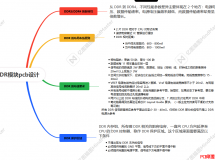
1. PCB 分类
$ }3 [, ]" K3 G+ ]3 c% B/ ^( \# H7 i2. PCB 材料 L, d. T+ Z! x. M
3. PCB 生产流程/ l" ]! r. Q" d$ j }( n
4. 水处理8 K; `6 a }% x, ^+ v, z
5. PCB 检验
& x/ f0 L0 p3 r0 j# c5 N6. 主要设备
3 R) {! Q/ Z6 a. C: a9 V7. 工程设计
3 Y" C; j( o( \( Q2 b8. 元器件组装( i5 x. U, V' u6 Q
1.PCB Sort (PCB 分类):$ K: n( L* H2 m- j$ m9 [
Single sided board(单面板) Double sided Board(双面板) Multilayer Board(多层板)Rigid board(刚性板)
/ B; |7 Q4 [5 @" U flexible board(挠性板) flex-rigid board(刚挠结合板) metal base PCB(金属基板) Blind board(盲孔板)
3 Z: t! R C5 D7 d O$ m2 iburied board(埋孔板) bare board(裸板)Quick turn prototype(样板)
6 Y) p, ?+ \3 h2.PCB Material(PCB 材料):( j V9 T& v; W; x; N
Copper clad laminate(CCL)(覆铜板) PREPREG(半固化片) Epoxy resin(环氧树脂) Copper foil(铜箔)
3 ]" {' s5 D5 v1 w7 NPTFE (Polytetralluoetylene) Teflon(聚四氟乙烯) dielectric constant(介电常数)Flexible copper clad(挠性覆铜板) silver film(银盐片) diazo film(重氮片)Solder mask(阻焊) Dry film(干膜) legend ink(字符油墨) " G S( O# D' S
peelable solder mask(可剥离阻焊) flux(助焊剂) additive(添加剂)6 P9 r5 t0 [4 o1 }) q
3.PCB Process(PCB 生产流程) :2 F2 N: i1 `" _+ n$ C% ~5 B
Wet process(湿法流程) Dry process(干法流程): {# f& ^# y, I. q3 ?% i* d. Y
FOR MULTILAYER MANUFACTURE PROCESS(多层线路板生产流程):Laminate cut(覆铜板) scrubbing(擦板) Image transfer(图形转移) internal layer(内层) Exposure(曝光) Developing(显影) ETCHING(蚀刻)
; k" \3 v) Q1 n% e* p/ ]+ y- L% _" Mblack / brown oxygen(黑/棕化) lay up(叠层) Laminating(层压) Drilling(钻孔) scrubbing(擦板)
) ]3 f2 o4 }. x7 l3 d, fPlated throughhole(孔金属化) PTH panel plating(板面电镀) pattern plating (plated resist) (图形电镀)
4 T4 Y, m+ }% T; HEtching(蚀刻)Inspection(检验) Printing solder mask(阻焊印刷) Exposure(曝光) Developing(显影)
2 a2 j$ M2 D# u. {Hot Cured(热固化) Hot Air Leveling(热风整平) IMMERSION GOLD(沉金)
; Y/ [. E8 |* |6 ePrinting legend ink (silkscreen printing)(字符印刷)Hot Cured(热固化) Routing(铣外形)
! A. \& z' D* l* c( s Jpunch(冲孔) Bare board testing(裸板测试) Final Inspection(终检) Packing(包装) Delivery(发货)6 ?* A5 z& J. o- d: r2 r
4.Water treatment(水处理)
) Z. W4 Y; R5 i- L7 @$ W3 s* L8 ADI (dialysis ion) water(去离子水) Waste watertreatment(污水处理) humidity (湿度)temperature(温度)
2 P; m g ^$ v/ F5.PCB Inspection(PCB 检验):
- w) s( {" h$ K. _3 vInspection standard(检验标准) defect open(开路)short(短路)measling(白斑)fibre exposure(漏基材) hole breakout(破孔) flatness(平面度) peelstrength(剥离强度) thermal shock(热冲击)2 F# i7 ~4 S6 y# U& `1 \) X7 F
thermalstress(热应力) Reworking(返工) manufacture panel(制造拼板) light integrator(光积分仪) stepscale(光尺) undercut factor(侧蚀系数) microetching(微蚀) over etching(过蚀)8 Z }5 Z9 D/ k5 d7 V/ K1 a! f
swimming(滑移) - ^( L2 Z9 Y# c+ ~# D) {
% c: n' u& O+ l. N+ u9 C
6.Major equipments(主要设备):
5 l0 C: V# S/ E( MLaser plotter(激光光绘机) CNC drilling machine(数控钻床) CNC routing machine(数控铣床)
' d* i( N. b; }1 [Scrubber(擦板机) Auto through hole plating line(自动沉铜线)panel plating line(板面电镀线) - x% V& y9 V9 G* t: n8 s
pattern plating line(plated resist) (图形电镀线) dry film laminator(贴膜机) Exposure(曝光机) : S- D# S, M8 X+ R! W) |: m
developing line(显影线) Etching line(蚀刻线) Auto registration punch(冲孔机) & A H8 A, q4 R8 G& m' l( }
Multilayer press system(多层板层压系统) Blackoxidation line(黑化线)
. l3 s, ?/ X8 F/ ~Automatic optical instrumentAOI(自动光学检测仪) Flying Probe test FPT(飞针检测仪)
# g# m7 Z6 `3 D" ? bHot air leveling(热风整平机) Impedancecontrol test system(阻抗控制检测仪)0 C% C7 G: r( h: u) d" C
7.Engineering Design(工程设计):! B% K# I' w4 c# w3 F5 S2 F
lay out(布线) CAD (computer aided design) (计算机辅助设计)
: h! _% c1 y6 W1 a- ^+ }CAM (computer aided manufacture) (计算机辅助制造)
9 v& x% s9 Z f8 L& Z! aEDA (Electronic design automatic) (电子设计自动化) origin(原点) mirroring(镜相)
' ^; r! z2 q+ hscalingfactor(比例系数) network(网络) conductor track(导线) PAD(焊盘) width(宽度)
+ Z$ W. j Z2 v4 }gap spacing(间隙) aperture(光圈) round(圆形) oblong(长圆形)square(正方形)
$ g+ U# F+ S; jrectangle(长方形) tear pad(泪滴焊盘) isolation pad(隔离焊盘) thermal pad(热焊盘)
^/ y4 Y- z+ D% _1 q) m! pmounting hole(安装孔) via(过孔) Plating throughhole PTH(金属化孔) NPTH(非金属化孔) 9 d! j# a+ V+ t2 T& ]4 E5 v
tooling hole(定位孔) Fiducial (基准点、反光点) layer to layerspacing(层间距) 6 w' f# u! U- Q! ]
layer Building up drawing(层叠图) external layer(外层) internal layer(内层)power layer(电源层) ground layer(接地层) signalline(信号线) target(标靶) slot(槽孔)
: k( V' b' B9 R7 I) u9 P+ M# y5 | tabconnector (golden finger) (金手指) Impedancecontrol PCB(阻抗控制) Golden board(黄金板)
7 R/ |/ Z! T7 q/ x: |& t/ @9 pMI(manufacture information) (制造说明) NOPE ( noprocess engineering ) (重订单)
+ C) Y/ {" Q& ~- I2 n5 \! a+ y# vphoto plotting(laser plotting)(激光光绘) positive(正片) negative(负片) p* ]2 r* Y0 I" e9 W8 [6 Y, e: }
8.Component Assembly(元器件组装):
' w7 l' d4 K$ o. v" l4 rsmt (Surface mount technology) (表面贴装技术) Bonding(邦定)
1 U1 S; v. z4 B% C% G! ]# S4 RDIP(dual inline package) (双列直插封装) QFP(quad flat package) (四面扁平封装)
+ D- O! w" V* HBGA(ballgrid array ) (球栅封装) SMD (Surface mount devices) (表面贴装设备)Placement machine(贴装机)
8 p& {% n/ d' X- J( b5 K4 iREFOLW SOLDERING(回流焊) WAVE SOLDERING(波峰焊)
t# D( \& A2 ~) {5 F 详情可见www.sz-jlc.com/s
% |2 ^# F% a4 P+ C& D5 `2 M$ y b' f8 @( R5 a. `4 |6 ~
|
|


 窥视卡
窥视卡

 置顶卡
置顶卡 变色卡
变色卡