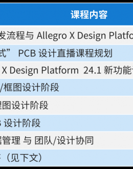
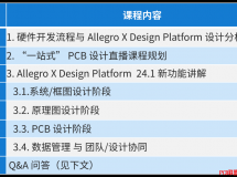
|
|
1、 主面:primary side
: B, K: U- W' k" \1 _3 T2、 辅面:secondary side( _! u# `1 n, X1 k- r
3、 支撑面:supporting plane
# Z* _1 x) f2 B0 |4、 信号:signal) g' s" z5 Y$ A, k# ~' o
5、 信号导线:signal conductor
) S6 B7 C% V$ j% w- Z3 t6、 信号地线:signal ground
H) U3 T6 Q7 b* P6 l7、 信号速率:signal rate1 K/ F( t$ c) w/ N
8、 信号标准化:signal standardization6 _8 @6 F# w7 k# R
9、 信号层:signal layer
) q1 J, o& r5 K$ R10、 寄生信号:spurious signal
1 F7 w& W* u3 |- ~! x: G11、 串扰:crosstalk; l6 h, n/ b% S0 `2 p, p9 }
12、 电容:capacitance
# z" _2 v! y+ E1 e13、 电容耦合:capacitive coupling# c+ a4 G6 c+ j3 b
14、 电磁干扰:electromagnetic interference
' [7 J0 A) m8 n, i, W% ]15、 电磁屏蔽:electromangetic shielding3 X' d8 R( {" w8 C# m
16、 噪音:noise* o7 t( M0 l( E" z# B8 d
17、 电磁兼容性:electromagnetic compatbility4 l7 Y! z& c4 V/ W1 a- S
18、 特性阻抗:impedance7 `! i7 C2 m$ a$ c
19、 阻抗匹配:impedance match: C8 M$ W" |( |5 Y# ?
20、 电感:inductance3 e1 E, w6 D4 E; Y" w
21、 延迟:delay
' E* v! q, z5 W8 _' Y+ Q22、 微带线:microstrip" x5 @; ~$ }" e4 J& W$ n& Z+ k
23、 带状线:stripline( j% e: W! }# z0 W' Z
24、 探测点:probe point6 e- n& K( J$ F; O+ S% _9 _" x
25、 开窗口:cross hatching! |( s/ M" ]+ ~- S" G9 v+ S n) V
26、 跨距:span
# b$ M! H2 Z9 k3 @5 `7 p8 i$ T& _27、 共面性(度):coplanarity
, y: I7 I; M. D5 v N4 y3 @# V28、 埋入电阻:buried resistance7 {0 \1 K6 J, E, n
29、 黄金板:golden board
! L' T' D$ U7 W4 ]" \, x3 [30、 芯板:core board
5 D% P5 k/ E3 Q+ d! b, s$ L5 v' L31、 薄基芯:thin core
! b% f" K! \7 \5 r: `" u32、 非均衡传输线:unbalanced transmission line W6 q/ ^: D9 L k0 T& A
33、 阀值:threshold
8 H Z C8 V: x# a' j+ _34、 极限值:threshold limit value(TLV)
- G9 U3 m5 c4 W+ _- r: E% F35、 散热层:heat sink plane9 j2 s: }# W5 R4 k! Q8 N, q# ^
36、 热隔离:heat sink plane
7 V( v. y3 U. O: E# Z9 T37、 导通孔堵塞:via filiing# ]& J1 H3 d) [" Q
38、 波动:surge( i! Q7 p7 @: A( E2 g7 u$ ?) w5 ]
39、 卡板:card0 z0 E: z, a0 @
40、 卡板盒/卡板柜:card cages/card racks
6 Y) j" x& t0 r; [$ U; C( }41、 薄型多层板:thin type multilayer board1 M1 R8 k- b! \: [ U; j2 E) o
42、 埋/盲孔多层板:
5 S; e O6 ]2 {7 e% g43、 模块:module# c; j5 V" ]4 N' @& p
44、 单芯片模块:single chip module (SCM)) M! z4 m2 z( `5 X# }
45、 多芯片模块:multichip module (MCM)
1 ~& f/ O: ?3 i& f) K46、 多芯片模块层压基板:laminate substrate version of multichip module (MCM-L)& c- D l5 m3 L0 Y
47、 多芯片模块陶瓷基数板:ceramic substrate version o fmultichip module (MCM-C)1 g _' d/ w; {* n0 T
48、 多芯片模块薄膜基板:deposition thin film substrate version of multilayer module (MCM-D)* I, i N" U) g6 w: [ D
49、 嵌入凸块互连技术:buried bump interconnection technology (B2 it); W+ G5 \; c+ h+ L
50、 自动测试技术:automatic test equipment (ATE)
: Z0 T0 c8 U( A1 A/ _' B. S51、 芯板导通孔堵塞:core board viafilling
* C. J( B* G- c9 P& h52、 对准标记:alignment mark
; N% D; |. l3 k! c. ^( b5 B2 U53、 基准标记:fiducial mark" [' X K3 O% q4 z
54、 拐角标记:corner mark3 N, q6 p- P- f7 K4 [) {: B
55、 剪切标记:crop mark
0 `' V5 f2 t) s6 \, X( v56、 铣切标记:routing mark
. o. G5 B5 ~* @" Y& N% |# }% E+ d57、 对位标记:registration mark V* m! E/ G8 I' o) f
58、 缩减标记:reduvtion mark
3 {; `6 b$ Q( s( H2 Y: W W2 H59、 层间重合度:layer to layer registration2 c% O0 q- [, y% P' f, B
60、 狗骨结构:dog hone+ O. M. W: Q* N* A3 K6 ~8 t
61、 热设计:thermal design
2 B& H. W! T; T K' g8 Y62、 热阻:thermal resistance
, c. M5 l. |( q* b |
|


 窥视卡
窥视卡


 置顶卡
置顶卡 变色卡
变色卡